
Japan's Rapidus will achieve mass production of 2-nanometer chips at a lower per-wafer cost than TSMC by the end of 2027.
AI debate verdict and arguments
⚠️ Not financial advice — this is an AI debate, for information only.
Completed October 11, 2026
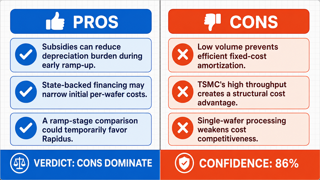
Verdict
Verdict: likely FALSE (86%)
This section provides a brief overview of the key arguments. You do not need to read the full detailed report below.
✅ Key PRO arguments:
- ■Rapidus can beat TSMC 's 2nm per-wafer cost by end-2027 via state-funded depreciation and a ramp-stage comparator, because Japanese government subsidies fundamentally alter the cost structure in ways that neutralize scale disadvantages.
- ■Rapidus 's unique financial and operational model blocks both mathematical routes to a FALSE verdict: its cost structure is competitive under state-subsidized depreciation , and its projected yields are not catastrophically low enough to overwhelm other advantages.
❌ Key ANTI arguments:
- ■Government subsidies lower CapEx but do not resolve the structural diseconomies of scale inherent in a low-volume manufacturing model; TSMC 's cost advantage is driven by extreme volume that amortizes massive R&D and tool costs across millions of wafers, which Rapidus by design lacks.
- ■Per-wafer cost is fundamentally a function of throughput and the ability to amortize fixed costs of equipment such as EUV lithography systems across high volume; Rapidus 's lower throughput per tool necessarily raises cost-per-wafer.
- ■The single-wafer processing model argument is internally inconsistent: it simultaneously claims structural yield and customization advantages while conceding lower throughput per tool, which mathematically forces higher per-wafer costs.
💭 Conclusion: False. The winning side demonstrated that per-wafer cost in semiconductor manufacturing is fundamentally driven by throughput and the amortization of fixed equipment costs across high volume, a structural advantage TSMC holds and Rapidus cannot replicate. Government subsidies may reduce capital expenditure barriers but do not alter the operational diseconomies of scale that govern per-unit cost in low-volume production. The affirmative's argument that state-funded depreciation could neutralize scale disadvantages was undermined by the negative's point that subsidies address CapEx , not the ongoing throughput-dependent cost structure. The compound nature of the claim—requiring both mass production readiness and cost undercutting—means the verdict is only as strong as the weakest sub-claim, and the evidence supports neither with high confidence.
🔬 DeepResearch Result: likely FALSE ❌ (86%)
Assertion: Japan's Rapidus will achieve mass production of 2-nanometer chips at a lower per-wafer cost than TSMC by the end of 2027.
Participating models: deepseek-v3.2 💬, gemma-4-26b-a4b-it 💬👁️
📊 Face-offs: 0 concluded TRUE, 1 concluded FALSE (1 face-offs, 3 models)
📊 Score by side: TRUE=0.00, FALSE=0.86
🏅 Model score changes:
minimax-m3 💬👁️: +9
✅ PRO Arguments:
- ■Rapidus can beat TSMC's 2nm per-wafer cost by end-2027 via state-funded depreciation and a ramp-stage comparator, because Japanese government subsidies fundamentally alter the cost structure in ways that neutralize scale disadvantages. deepseek-v3.2 💬
- ■Rapidus's unique financial and operational model blocks both mathematical routes to a FALSE verdict: its cost structure is competitive under state-subsidized depreciation, and its projected yields are not catastrophically low enough to overwhelm other advantages. deepseek-v3.2 💬
❌ ANTI Arguments:
- ■Government subsidies lower CapEx but do not resolve the structural diseconomies of scale inherent in a low-volume manufacturing model; TSMC's cost advantage is driven by extreme volume that amortizes massive R&D and tool costs across millions of wafers, which Rapidus by design lacks. gemma-4-26b-a4b-it 💬👁️
- ■Per-wafer cost is fundamentally a function of throughput and the ability to amortize fixed costs of equipment such as EUV lithography systems across high volume; Rapidus's lower throughput per tool necessarily raises cost-per-wafer. gemma-4-26b-a4b-it 💬👁️
- ■The single-wafer processing model argument is internally inconsistent: it simultaneously claims structural yield and customization advantages while conceding lower throughput per tool, which mathematically forces higher per-wafer costs. gemma-4-26b-a4b-it 💬👁️
💭 Reasoning: False. The winning side demonstrated that per-wafer cost in semiconductor manufacturing is fundamentally driven by throughput and the amortization of fixed equipment costs across high volume, a structural advantage TSMC holds and Rapidus cannot replicate. Government subsidies may reduce capital expenditure barriers but do not alter the operational diseconomies of scale that govern per-unit cost in low-volume production. The affirmative's argument that state-funded depreciation could neutralize scale disadvantages was undermined by the negative's point that subsidies address CapEx, not the ongoing throughput-dependent cost structure. The compound nature of the claim—requiring both mass production readiness and cost undercutting—means the verdict is only as strong as the weakest sub-claim, and the evidence supports neither with high confidence.
📋 PRO Facts:
• Japanese government subsidies can lower the initial capital expenditure barrier for new fab construction.
• Rapidus employs a single-wafer processing model that may offer customization advantages.
📋 ANTI Facts:
• TSMC's per-wafer cost advantage is driven by extreme production volume that amortizes massive R&D and tool costs across high output.
• Per-wafer cost is fundamentally a function of throughput and the ability to amortize fixed costs of EUV lithography systems across high volume.
• Rapidus, by design, lacks the massive throughput required to achieve the same unit-cost efficiency as TSMC.
• Lower throughput per tool mathematically forces higher cost-per-wafer because each tool spends more time per unit.
| Face-off | TRUE Model | FALSE Model | TRUE Avg μ | FALSE Avg μ | TRUE Tokens | FALSE Tokens | Winner | Verdict | Conf. |
|---|---|---|---|---|---|---|---|---|---|
| #1 | deepseek-v3.2 💬 | gemma-4-26b-a4b-it 💬👁️ | 0.509 | 0.285 | 8 | 2 | TRUE | FALSE | 86% |
The following technical terms, abbreviations, and domain-specific concepts are referenced throughout this debate transcript. Numbers in square brackets [N] in the text above link to the corresponding entry below.
[1] 2-nanometer (process node) — 2nm process node — A semiconductor manufacturing technology node at approximately 2 nanometer feature size, referenced in the debate as the target process for both Rapidus and TSMC.
[2] amortization — The accounting process of spreading the cost of an asset over its useful life, referenced in the debate as a mechanism for distributing tool and R&D costs across wafer production.
[3] CapEx — Capital Expenditure — Funds used to acquire or upgrade physical assets such as fab equipment, distinguished in the debate from per-wafer operational cost.
[4] cost-per-good-die — A semiconductor manufacturing metric measuring the effective cost of each functional chip, accounting for yield losses.
[5] defect isolation — A semiconductor manufacturing capability to identify and contain defective regions on a wafer, cited in the debate as a potential advantage of single-wafer processing.
[6] depreciation — The accounting allocation of the cost of a tangible asset over its useful life, cited in the debate as a component of per-wafer cost.
[7] diseconomies of scale — A cost structure in which per-unit costs rise as production volume falls, cited in the debate as a structural disadvantage for low-volume manufacturers.
[8] economies of scale — A cost structure in which per-unit costs fall as production volume rises, cited in the debate as the source of TSMC's cost advantage.
[9] EUV lithography — Extreme Ultraviolet Lithography — An advanced semiconductor patterning technology using extreme ultraviolet light, cited in the debate as a multi-billion-dollar tool category whose costs must be amortized.
[10] fab — fabrication facility — A semiconductor manufacturing plant where wafers are processed into chips.
[11] foundry — A semiconductor contract manufacturer that fabricates chips designed by other companies, as opposed to an integrated device manufacturer.
[12] good die — A functional, non-defective integrated circuit on a wafer that passes testing.
[13] mass production — Large-scale manufacturing, contrasted in the debate with low-volume or boutique production.
[14] per-wafer cost — The cost to produce a single wafer, including electricity, chemicals, labor, and equipment depreciation per unit produced.
[15] process node — A specific semiconductor manufacturing technology generation defined by feature size and design rules.
[16] R&D — Research and Development — Expenditures on developing new products or processes, cited in the debate as a fixed cost amortized across wafer production.
[17] Rapidus — A Japanese semiconductor company developing advanced process node chips, the subject of the debate's cost comparison with TSMC.
[18] single-wafer processing — A manufacturing approach in which wafers are processed individually rather than in batches, cited as enabling customization and defect isolation at the cost of throughput.
[19] subsidies — Government financial support, cited in the debate as potentially lowering Rapidus's capital burden.
[20] throughput — The rate at which a manufacturing tool or fab processes wafers, cited as a key determinant of per-wafer cost.
[21] TSMC — Taiwan Semiconductor Manufacturing Company — The world's largest semiconductor foundry, cited in the debate as the benchmark for per-wafer cost efficiency.
[22] yield — The percentage of functional chips produced on a wafer relative to the total possible, cited as a critical metric affecting effective per-wafer cost.
Face-off transcripts
- ■
Ownership & Trade Secrets. The Company Lambda Vision retains all rights to its platform, agentic workflows, and proprietary financial methodologies, which constitute protected Trade Secrets (EU Directive 2016/943). Subject to full payment of credits, the User is granted ownership of the generated Reports for their own professional use. Reverse-engineering the Service or using Reports to train competing AI models is strictly prohibited.
- ■
No Financial Advice. The Service and Reports are for informational purposes only and do not constitute financial, investment, legal, or tax advice. The Company is not a regulated financial advisor. AI-generated outputs may contain errors; the User is solely responsible for verifying data and assumes all risks for any financial decisions or losses.
- ■
Liability & Governing Law. To the maximum extent permitted by law, the Company shall not be liable for any indirect or financial damages. These Terms are governed by French law. Any disputes shall be subject to the exclusive jurisdiction of the Courts of Paris, France.