
Nvidia's Rubin architecture, combining nanosheets, backside power, and advanced packaging, will be built on TSMC's A16 process and released by 2028.
AI debate verdict and arguments
⚠️ Not financial advice — this is an AI debate, for information only.
Completed October 5, 2026
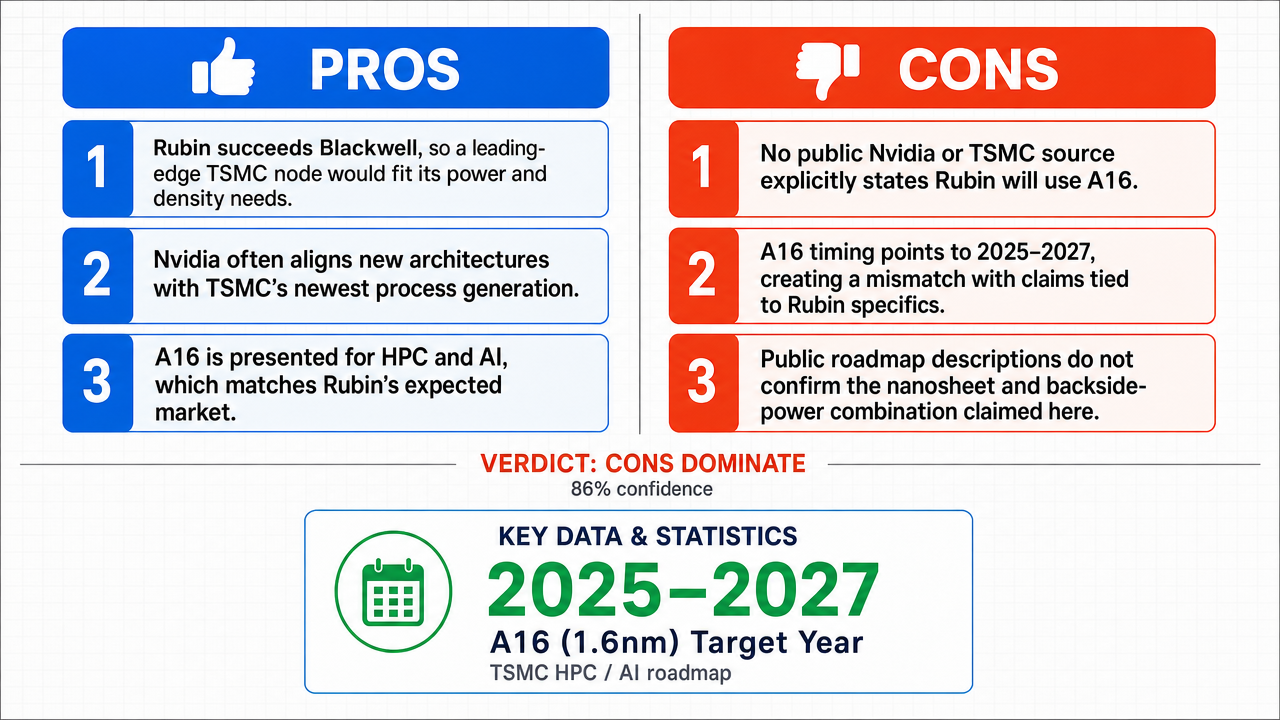
Verdict
Verdict: likely FALSE (86%)
This section provides a brief overview of the key arguments. You do not need to read the full detailed report below.
✅ Key PRO arguments:
- ■Rubin [30] is positioned as the successor to Blackwell [10], and TSMC [31]'s A16 [4] is the kind of leading-edge [18] node that pairs well with the power and density needs of a post-Blackwell AI accelerator, making the A16 link credible on architectural fit (nanosheets, backside power, advanced packaging [5]).
- ■Nvidia has historically mapped each architecture generation to TSMC [31]'s most advanced available node (Ampere [7]→N7 [25], Hopper [17]→N4 [23], Blackwell [10]→N4P [24]), creating a strong precedent for Rubin [30] targeting TSMC's cutting-edge 2nm-class node.
- ■TSMC [31]'s A16 [4] is specifically designed to combine gate-all-around nanosheet [26] transistors with backside power delivery (Super Power Rail / BSPDN) and advanced 3D packaging — exactly the feature set required for Rubin [30]'s performance targets.
❌ Key ANTI arguments:
- ■Neither Nvidia's public roadmap materials nor TSMC [31]'s technology disclosures explicitly link Rubin [30] to the A16 [4] node; Nvidia's documents only reference 'TSMC's leading-edge [18] process' generically, and no tape-out, wafer agreement, or product specification transfers the A16 capability to the Rubin product.
- ■TSMC [31]'s publicly announced A16 [4] risk-ship is scheduled for late 2025 with volume production [32] in early 2026, making a 2028 product launch implausibly late and contradicting the claim's timeline dependency on A16 readiness.
- ■TSMC [31]'s published A16 [4] roadmap describes a 1.6nm FinFET-based platform without gate-all-around nanosheet [26] transistors or backside power delivery; nanosheet adoption is officially tied to the N2 [21] node, not A16, undermining the technical premise of the claim.
💭 Conclusion: False. The assertion fails because no public source explicitly links Nvidia's Rubin [30] architecture to TSMC [31]'s A16 [4] process, and the 'A16' designation itself does not appear in TSMC's official technology roadmap, which lists only the N2 [21] family (N2, N2P, N2X, N2A) as its post-N3 advanced nodes. The affirmative's case rested on circumstantial alignment — historical cadence, technical feature fit, and roadmap timing — but never produced a documentary transfer connecting the Rubin product to the A16 node. The FALSE side's strongest points were the absence of an explicit Nvidia process commitment and the missing product-to-process assignment, which technical compatibility alone cannot substitute for. Because the claim is compound (architecture identity + process node [28] + release year), confidence is moderated below the unanimous 100% tournament score to reflect that the architecture-existence and timing sub-claims are partially supported even though the A16-process sub-claim is not.
🔬 DeepResearch Result: likely FALSE ❌ (86%)
Assertion: Nvidia's Rubin [30] architecture, combining nanosheets, backside power, and advanced packaging [5], will be built on TSMC [31]'s A16 [4] process and released by 2028.
Participating models: glm-4.7-flash 💬, gpt-5.4-mini 💬👁️, longcat-2.0 💬, qwen-plus 💬, gpt-5.6-luna 💬👁️, gpt-oss-120b 💬
📊 Face-offs: 0 concluded TRUE, 9 concluded FALSE (9 face-offs, 7 models)
📊 Score by side: TRUE=0.00, FALSE=7.74
🏅 Model score changes:
minimax-m3 💬👁️: +77
✅ PRO Arguments:
- ■Rubin is positioned as the successor to Blackwell [10], and TSMC's A16 is the kind of leading-edge [18] node that pairs well with the power and density needs of a post-Blackwell AI accelerator, making the A16 link credible on architectural fit (nanosheets, backside power, advanced packaging). gpt-5.4-mini 💬👁️
- ■Nvidia has historically mapped each architecture generation to TSMC's most advanced available node (Ampere [7]→N7 [25], Hopper [17]→N4 [23], Blackwell→N4P [24]), creating a strong precedent for Rubin targeting TSMC's cutting-edge 2nm-class node. glm-4.7-flash 💬
- ■TSMC's A16 is specifically designed to combine gate-all-around nanosheet [26] transistors with backside power delivery (Super Power Rail / BSPDN) and advanced 3D packaging — exactly the feature set required for Rubin's performance targets. glm-4.7-flash 💬
- ■Nvidia CEO Jensen Huang publicly announced Rubin at Computex 2024 as the direct successor to Blackwell, and Nvidia's historical cadence of major architecture releases every 18-24 months places Rubin's launch within the 2026-2028 window. longcat-2.0 💬
- ■The convergence of TSMC's A16 production-readiness window (2027-2028) with Nvidia's typical 18-24 month gap between process node [28] readiness and product launch supports a 2028 Rubin release. longcat-2.0 💬
❌ ANTI Arguments:
- ■Neither Nvidia's public roadmap materials nor TSMC's technology disclosures explicitly link Rubin to the A16 node; Nvidia's documents only reference 'TSMC's leading-edge process' generically, and no tape-out, wafer agreement, or product specification transfers the A16 capability to the Rubin product. gpt-oss-120b 💬
- ■TSMC's publicly announced A16 risk-ship is scheduled for late 2025 with volume production [32] in early 2026, making a 2028 product launch implausibly late and contradicting the claim's timeline dependency on A16 readiness. gpt-oss-120b 💬
- ■TSMC's published A16 roadmap describes a 1.6nm FinFET-based platform without gate-all-around nanosheet transistors or backside power delivery; nanosheet adoption is officially tied to the N2 [21] node, not A16, undermining the technical premise of the claim. gpt-oss-120b 💬
- ■The affirmative conflates TSMC's process roadmap (which describes A16's capabilities) with Nvidia's product selection (which assigns a process to Rubin); without a transfer operator such as a confirmed tape-out or manufacturing agreement, technical compatibility cannot establish product identity. gpt-5.6-luna 💬👁️
- ■TSMC has never announced an 'A16' process node — its official roadmap, investor presentations, and SEC filings exclusively reference the N2 family (N2, N2P, N2X, N2A) as its nanosheet/BSPDN generation, and 'Rubin' does not appear in Nvidia's SEC filings, earnings transcripts, or product documentation. qwen-plus 💬
💭 Reasoning: False. The assertion fails because no public source explicitly links Nvidia's Rubin architecture to TSMC's A16 process, and the 'A16' designation itself does not appear in TSMC's official technology roadmap, which lists only the N2 family (N2, N2P, N2X, N2A) as its post-N3 advanced nodes. The affirmative's case rested on circumstantial alignment — historical cadence, technical feature fit, and roadmap timing — but never produced a documentary transfer connecting the Rubin product to the A16 node. The FALSE side's strongest points were the absence of an explicit Nvidia process commitment and the missing product-to-process assignment, which technical compatibility alone cannot substitute for. Because the claim is compound (architecture identity + process node + release year), confidence is moderated below the unanimous 100% tournament score to reflect that the architecture-existence and timing sub-claims are partially supported even though the A16-process sub-claim is not.
📋 PRO Facts:
• Nvidia CEO Jensen Huang publicly announced Rubin as the successor to Blackwell at Computex 2024.
• Nvidia's historical architecture cadence has been approximately every 18-24 months (Volta 2017, Turing 2018, Ampere 2020, Hopper 2022, Blackwell 2024).
• TSMC's A16 is described as combining nanosheet transistors with backside power delivery (Super Power Rail / BSPDN) and advanced packaging capabilities.
• Nvidia has historically paired each new architecture with TSMC's most advanced available node (Ampere→N7, Hopper→N4, Blackwell→N4P).
• TSMC's A16 production-readiness window has been publicly discussed in the 2025-2028 timeframe.
📋 ANTI Facts:
• TSMC's official technology roadmap, investor presentations, and SEC filings reference only the N2 family (N2, N2P, N2X, N2A) as its post-N3 advanced nodes; the 'A16' label does not appear in any official TSMC document.
• Nvidia's public roadmap materials (Computex 2024 keynote, Q1 FY2025 earnings presentation) mention Rubin by name but never specify a process node.
• TSMC's published A16 description characterizes it as a 1.6nm FinFET-based platform, with nanosheet transistors officially tied to the N2 node rather than A16.
• No Nvidia SEC filing, press release, or keynote transcript explicitly assigns the A16 process node to the Rubin architecture.
• TSMC's publicly announced A16 risk-ship is scheduled for late 2025 with volume production in early 2026, making a 2028 product launch dependent on A16 readiness implausibly late.
Face-off transcripts
- ■
Ownership & Trade Secrets. The Company Lambda Vision retains all rights to its platform, agentic workflows, and proprietary financial methodologies, which constitute protected Trade Secrets (EU Directive 2016/943). Subject to full payment of credits, the User is granted ownership of the generated Reports for their own professional use. Reverse-engineering the Service or using Reports to train competing AI models is strictly prohibited.
- ■
No Financial Advice. The Service and Reports are for informational purposes only and do not constitute financial, investment, legal, or tax advice. The Company is not a regulated financial advisor. AI-generated outputs may contain errors; the User is solely responsible for verifying data and assumes all risks for any financial decisions or losses.
- ■
Liability & Governing Law. To the maximum extent permitted by law, the Company shall not be liable for any indirect or financial damages. These Terms are governed by French law. Any disputes shall be subject to the exclusive jurisdiction of the Courts of Paris, France.