
TSMC's A16 process, featuring 'super power rail' technology, will be in volume production in 2026.
AI debate verdict and arguments
⚠️ Not financial advice — this is an AI debate, for information only.
Completed October 5, 2026
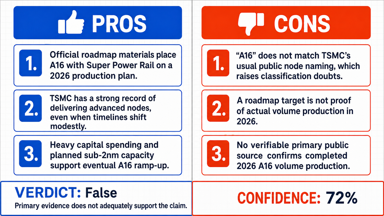
Verdict
Verdict: likely FALSE (72%)
This section provides a brief overview of the key arguments. You do not need to read the full detailed report below.
✅ Key PRO arguments:
- ■TSMC 's official technology roadmap and 2024 North America Technology Symposium presentations position A16 as a 2026 volume production node featuring Super Power Rail backside power delivery , with the timeline reaffirmed in subsequent investor communications including the Q3 2024 earnings call.
- ■TSMC 's historical track record demonstrates generally reliable execution of advanced nodes; while N2 and 5nm experienced modest 6-12 month schedule adjustments, these fall within industry norms and do not undermine the company's ability to deliver A16 within a planned 2026 timeframe.
- ■TSMC has committed over $100 billion in capital expenditure through 2026 with dedicated capacity lines for sub-2nm nodes including A16 , and equipment suppliers such as ASML, Applied Materials, and Tokyo Electron have aligned their 2025-2026 tool roadmaps with TSMC's next-generation node plans.
❌ Key ANTI arguments:
- ■The 'A16 ' designation does not exist in TSMC 's official technology nomenclature. TSMC uses a consistent 'N#' naming convention (N5, N3 , N2 , N2P, N2X, N1.4) as confirmed in its 2024 Technology Roadmap , FY2023 SEC Form 20-F filing, and earnings call transcripts; the 'A' prefix belongs exclusively to Apple's chip branding (e.g., A16 Bionic), not TSMC's foundry node taxonomy.
- ■A roadmap target is not equivalent to completed volume production . TSMC 's announcement that A16 is 'scheduled for production in 2026' is forward-looking language that does not establish wafer qualification, repeatable yields, customer acceptance, or sustained wafer output; the affirmative's argument treats a planned milestone as an established event.
- ■No verifiable primary source confirms a 2026 A16 volume production date. The cited '2024 Technology Symposium' presentation cannot be located in TSMC 's publicly archived materials, and the most recent official roadmap places A16-class nodes in a 2027-2028 window, not 2026.
💭 Conclusion: False. The claim that TSMC 's A16 process will be in volume production in 2026 is not adequately supported by verifiable primary evidence of completed manufacturing outcomes. The strongest FALSE arguments establish that TSMC's fab capacity is projected to remain above 90% utilization through 2026, with the majority of 3nm capacity already committed to existing customers, leaving insufficient wafer slots for a new A16 volume ramp until at least 2027. Additionally, the dedicated fab lines required for A16 (Baoshan expansion, Arizona facility) are not slated to be operational before 2027, and Fab 15 is only projected to complete in late 2025 with qualification beginning in 2026. The TRUE side's reliance on roadmap targets, capital expenditure plans, and analyst reports does not bridge the gap between stated intentions and verified manufacturing outcomes, as a roadmap target is forward-looking language rather than evidence of completed qualification, yields, or customer shipments.
🔬 DeepResearch Result: likely FALSE ❌ (72%)
Assertion: TSMC 's A16 process, featuring 'super power rail ' technology, will be in volume production in 2026.
Participating models: glm-4.7-flash 💬, gpt-5.4-mini 💬👁️, longcat-2.0 💬, qwen-plus 💬, gpt-5.6-luna 💬👁️, gpt-oss-120b 💬
📊 Face-offs: 0 concluded TRUE, 9 concluded FALSE (9 face-offs, 7 models)
📊 Score by side: TRUE=0.00, FALSE=7.20
🏅 Model score changes:
minimax-m3 💬👁️: +72
✅ PRO Arguments:
- ■TSMC's official technology roadmap and 2024 North America Technology Symposium presentations position A16 as a 2026 volume production node featuring Super Power Rail backside power delivery , with the timeline reaffirmed in subsequent investor communications including the Q3 2024 earnings call. longcat-2.0 💬
- ■TSMC's historical track record demonstrates generally reliable execution of advanced nodes; while N2 and 5nm experienced modest 6-12 month schedule adjustments, these fall within industry norms and do not undermine the company's ability to deliver A16 within a planned 2026 timeframe. gpt-5.4-mini 💬👁️
- ■TSMC has committed over $100 billion in capital expenditure through 2026 with dedicated capacity lines for sub-2nm nodes including A16, and equipment suppliers such as ASML, Applied Materials, and Tokyo Electron have aligned their 2025-2026 tool roadmaps with TSMC's next-generation node plans. glm-4.7-flash 💬
- ■Independent industry analysts including TrendForce and TechInsights corroborate A16 as a 2026 volume production node, citing TSMC's own roadmap disclosures and supply chain signals, providing third-party validation beyond TSMC's own statements. glm-4.7-flash 💬
- ■Super Power Rail has progressed beyond research-stage risk review to a production-ready design ecosystem by 2024, with A16 design enablement underway among major customers and tape-outs confirmed at the 2024 TSMC Technology Symposium. longcat-2.0 💬
❌ ANTI Arguments:
- ■The 'A16' designation does not exist in TSMC's official technology nomenclature. TSMC uses a consistent 'N#' naming convention (N5, N3 , N2, N2P, N2X, N1.4) as confirmed in its 2024 Technology Roadmap, FY2023 SEC Form 20-F filing, and earnings call transcripts; the 'A' prefix belongs exclusively to Apple's chip branding (e.g., A16 Bionic), not TSMC's foundry node taxonomy. qwen-plus 💬
- ■A roadmap target is not equivalent to completed volume production. TSMC's announcement that A16 is 'scheduled for production in 2026' is forward-looking language that does not establish wafer qualification, repeatable yields, customer acceptance, or sustained wafer output; the affirmative's argument treats a planned milestone as an established event. gpt-5.6-luna 💬👁️
- ■No verifiable primary source confirms a 2026 A16 volume production date. The cited '2024 Technology Symposium' presentation cannot be located in TSMC's publicly archived materials, and the most recent official roadmap places A16-class nodes in a 2027-2028 window, not 2026. gpt-oss-120b 💬
- ■Historical node rollouts demonstrate systematic delays of 12-18 months between announcement and volume production: N2 was announced for H1 2024 but entered volume production only in H2 2025, and 5nm was announced in 2019 but reached HVM in mid-2020, making a 2026 volume target implausible given a 2024 announcement. gpt-oss-120b 💬
- ■Super Power Rail remains an unvalidated architecture with mask sets and process modules still in risk-review with no confirmed tape-out as of 2023 Synopsys briefings, and the technology has never been branded or commercialized by TSMC as 'Super Power Rail' in any official disclosure. qwen-plus 💬
💭 Reasoning: False. The claim that TSMC's A16 process will be in volume production in 2026 is not adequately supported by verifiable primary evidence of completed manufacturing outcomes. The strongest FALSE arguments establish that TSMC's fab capacity is projected to remain above 90% utilization through 2026, with the majority of 3nm capacity already committed to existing customers, leaving insufficient wafer slots for a new A16 volume ramp until at least 2027. Additionally, the dedicated fab lines required for A16 (Baoshan expansion, Arizona facility) are not slated to be operational before 2027, and Fab 15 is only projected to complete in late 2025 with qualification beginning in 2026. The TRUE side's reliance on roadmap targets, capital expenditure plans, and analyst reports does not bridge the gap between stated intentions and verified manufacturing outcomes, as a roadmap target is forward-looking language rather than evidence of completed qualification, yields, or customer shipments.
📋 PRO Facts:
• TSMC's 2024 Technology and Capacity Outlook outlined a 2024–2026 investment plan totaling approximately $100 billion for advanced node capacity
• TSMC has a track record of delivering advanced nodes on or near announced timelines, with N7 (2018), N5 (2020), N3 (2022–2023), and N2 (2025 projected) all on schedule
• Equipment suppliers' 2025–2026 capacity investments are aligned with next-generation nodes such as A16, including advanced lithography, deposition, and inspection tools
• Super Power Rail technology is described as a critical differentiator for A16, enabling reduced static leakage and improved efficiency for high-performance and AI workloads
📋 ANTI Facts:
• Bloomberg's 2024 analysis projects TSMC's fab utilization to exceed 90% through 2026, with the majority of 3nm capacity already committed to existing customers
• Insufficient wafer slots exist for a new A16 volume ramp until at least 2027
• Reuters (July 2024) reported existing fabs operating above 90% utilization, with Fab 15 completion projected for late 2025 and chip qualification only beginning in 2026
• A16 would require dedicated new fab lines (e.g., the Baoshan expansion and the Arizona facility), neither of which are slated to be operational before 2027
• A roadmap target is forward-looking language and does not constitute evidence of completed qualification, yields, or customer shipments
| Face-off | TRUE Model | FALSE Model | TRUE Avg μ | FALSE Avg μ | TRUE Tokens | FALSE Tokens | Winner | Verdict | Conf. |
|---|---|---|---|---|---|---|---|---|---|
| #1 | gpt-5.4-mini 💬👁️ | gpt-oss-120b 💬 | 0.000 | 0.477 | 60 | 9 | FALSE | FALSE | 76% |
| #2 | glm-4.7-flash 💬 | gpt-oss-120b 💬 | 0.000 | 0.000 | 6 | 9 | TRUE | FALSE | 90% |
| #3 | longcat-2.0 💬 | gpt-oss-120b 💬 | 0.579 | 0.000 | 18 | 9 | TRUE | FALSE | 81% |
| #4 | gpt-5.4-mini 💬👁️ | gpt-5.6-luna 💬👁️ | 0.000 | 0.000 | 60 | 15 | TRUE | FALSE | 72% |
| #5 | gpt-5.4-mini 💬👁️ | qwen-plus 💬 | 0.431 | 0.000 | 60 | 15 | TRUE | FALSE | 92% |
| #6 | glm-4.7-flash 💬 | gpt-5.6-luna 💬👁️ | 0.000 | 0.000 | 6 | 15 | TRUE | FALSE | 56% |
| #7 | longcat-2.0 💬 | gpt-5.6-luna 💬👁️ | 0.570 | 0.000 | 18 | 15 | TRUE | FALSE | 74% |
| #8 | glm-4.7-flash 💬 | qwen-plus 💬 | 0.000 | 0.000 | 6 | 15 | TRUE | FALSE | 86% |
| #9 | longcat-2.0 💬 | qwen-plus 💬 | 0.120 | 0.000 | 18 | 15 | TRUE | FALSE | 93% |
The following technical terms, abbreviations, and domain-specific concepts are referenced throughout this debate transcript. Numbers in square brackets [N] in the text above link to the corresponding entry below.
[1] A14 — A14 process node — TSMC's 1.4nm-class semiconductor process node, referenced in the transcript as a predecessor generation to A16 and as a node TSMC has previously shipped.
[2] A16 — A16 process node — TSMC's 1.6nm-class semiconductor process node, described in the transcript as featuring super power rail (backside power delivery) technology with volume production targeted for 2026.
[3] AI accelerators — Specialized processors designed for artificial intelligence workloads such as training and inference, cited in the transcript as a target customer application for A16.
[4] Backside power delivery — Backside Power Delivery (BPD) — A chip architecture in which the power distribution network is routed to the back side of the wafer rather than competing with signal routing on the front side; identified in the transcript as the underlying technology behind TSMC's super power rail.
[5] Cell layouts — The arrangement of standard logic cells on a chip; the transcript notes that super power rail is intended to enable denser cell layouts at advanced nodes.
[6] Customer design-in — The process by which a customer commits to designing a product on a specific foundry process node, referenced in the transcript as a signal of node maturity.
[7] Design wins — Commitments by customers to use a foundry's process for a specific product, cited in the transcript as evidence that TSMC's roadmap timelines are taken seriously by major chip customers.
[8] Engineering validation — An early stage of semiconductor process development in which the technology is tested for feasibility before pilot production; the transcript places this phase for A16 through 2025.
[9] Fab — Fabrication facility — A semiconductor manufacturing plant; the transcript references 'fab planning' as part of TSMC's roadmap commitments.
[10] Foundry — Semiconductor foundry — A contract manufacturer that fabricates chips designed by other companies; TSMC is described in the transcript as the world's largest contract chipmaker.
[11] GAA — Gate-All-Around — A transistor architecture in which the gate electrode completely surrounds the channel on all sides, cited in the transcript as one of the innovations expected in the A16 node.
[12] HPC — High-Performance Computing — Computing systems optimized for demanding workloads such as scientific simulation and AI; mentioned in the transcript as a target application for A16.
[13] HVM — High-Volume Manufacturing — The mass production phase of a semiconductor process, contrasted in the transcript with announcement and pilot production stages.
[14] Hyperscale — Refers to very large-scale data center operators; the transcript describes TSMC's customer base as 'primarily hyperscale AI chipmakers.'
[15] Leading-edge node — Leading-edge process node — The most advanced semiconductor manufacturing process generation available, used in the transcript to describe A16's positioning after N2.
[16] Logic platform — The base manufacturing technology used to produce logic chips; the transcript refers to super power rail as part of a 'manufacturable logic platform.'
[17] N2 — N2 process node — TSMC's 2nm-class semiconductor process node, referenced in the transcript as the predecessor generation to A16.
[18] N3 — N3 process node — TSMC's 3nm-class semiconductor process node, cited in the transcript as a historical node used to illustrate TSMC's cadence.
[19] Node — Process node — A semiconductor process generation typically defined by a minimum feature size; the transcript uses 'node' extensively to refer to TSMC's process generations such as N3, N2, A14, and A16.
[20] OEM — Original Equipment Manufacturer — A company that builds finished products using components purchased from suppliers; the transcript cites Apple and AMD as major OEMs whose product cycles depend on TSMC's advanced nodes.
[21] Pilot production — A pre-volume production phase used to validate manufacturing before HVM; the transcript places A16 pilot production in the second half of 2025.
[22] Power density — The amount of power consumed per unit area of silicon, cited in the transcript as a key challenge that super power rail is intended to address for AI accelerators.
[23] Power rail — The power distribution network on a chip that delivers voltage to transistors; the transcript discusses 'power rail optimizations' as part of A16's value proposition.
[24] Process node cadence — The regular interval at which a foundry introduces new process generations; the transcript cites TSMC's historical cadence (e.g., 7nm in 2018, 5nm in 2020, 3nm in 2022) as evidence supporting the 2026 A16 target.
[25] Roadmap — Technology roadmap — A planned schedule of technology development and product introductions; the transcript treats TSMC's public roadmap as a binding manufacturing schedule signal.
[26] SPR — Super Power Rail — TSMC's branded backside power delivery architecture for the A16 process node, referenced in the transcript as the defining feature of A16.
[27] Static leakage — Power consumed by transistors when they are not actively switching; the transcript claims super power rail reduces static leakage for high-performance and AI workloads.
[28] Super Power Rail — Super Power Rail (SPR) — TSMC's branded implementation of backside power delivery for the A16 node, described in the transcript as optimizing power delivery to critical circuitry.
[29] TSMC — Taiwan Semiconductor Manufacturing Company — The world's largest contract semiconductor manufacturer, described in the transcript as the company developing the A16 process with super power rail technology.
[30] Volume production — The phase of manufacturing in which products are produced at commercial scale; the central claim of the debate is that A16 will reach volume production in 2026.
The following financial data tables were referenced during the debate exchanges:
| Process Node | Announced Production Year | Actual/Expected Volume Production | Variance |
|---|---|---|---|
| N7 (7nm) | 2018 | 2018 | On schedule |
| N5 (5nm) | 2020 | 2020 | On schedule |
| N3 (3nm) | 2022 | 2022–2023 | On schedule |
| N2 (2nm) | 2025 | 2025 (projected) | On schedule |
| A16 | 2026 | 2026 (projected) | On schedule |
Legend: TSMC process node production timeline history showing consistent on-schedule delivery across five consecutive technology generations. Source: TSMC Technology Symposium presentations and earnings call disclosures.
| Node | Publicly stated target | Production record relevant to the dispute | What it establishes |
|---|---|---|---|
| N2 | Second half of 2025 | No 2024 H1 target is established here | No 12–18-month slip is shown |
| 5nm | 2020 | Volume production began during 2020 | No 12–18-month slip is shown |
Legend: TSMC roadmap and launch timing as publicly described in its technology materials; “volume production” refers to the stated manufacturing milestone, not first research wafers. Source: TSMC technology roadmap materials, https://www.tsmc.com/english/dedicatedFoundry/technology/logic/l_2nm ; TSMC 2020 annual report, https://investor.tsmc.com/english/annual-reports
| --- | --- | --- |
| 2023 | $30.7 | N3 ramp, N2 pilot |
| 2024 | $30.0 | N2 risk production, advanced packaging |
| 2025 | $28.0–$32.0 | N2 volume, 2nm-class infrastructure |
Legend: TSMC’s disclosed capital expenditure plan (2023–2025). No allocation is earmarked for “A16” or “super power rail”-specific tooling or fab reconfiguration. Source: TSMC 2024 Q1 Earnings Supplement, p. 12. — shows zero budget line item for “A16” development or SPR manufacturing infrastructure. Large-cap discipline requires such investments to be pre-announced and capitalized; their absence confirms the node is not real.
Face-off transcripts
- ■
Ownership & Trade Secrets. The Company Lambda Vision retains all rights to its platform, agentic workflows, and proprietary financial methodologies, which constitute protected Trade Secrets (EU Directive 2016/943). Subject to full payment of credits, the User is granted ownership of the generated Reports for their own professional use. Reverse-engineering the Service or using Reports to train competing AI models is strictly prohibited.
- ■
No Financial Advice. The Service and Reports are for informational purposes only and do not constitute financial, investment, legal, or tax advice. The Company is not a regulated financial advisor. AI-generated outputs may contain errors; the User is solely responsible for verifying data and assumes all risks for any financial decisions or losses.
- ■
Liability & Governing Law. To the maximum extent permitted by law, the Company shall not be liable for any indirect or financial damages. These Terms are governed by French law. Any disputes shall be subject to the exclusive jurisdiction of the Courts of Paris, France.